
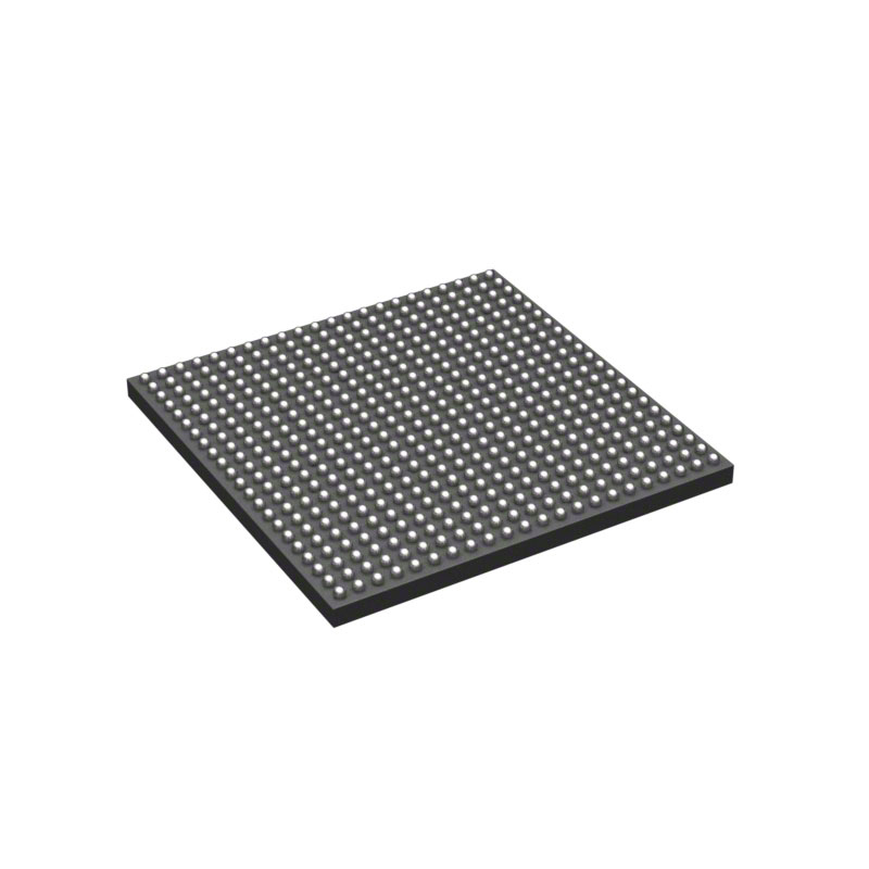
LFXP2-17E-5FN484I
High-density FPGA with 282,624 flip-flops
| 数量 | 単価(USD) | 合計金額 |
|---|---|---|
| 1 | $78.396 | $78.40 |
| 200 | $30.339 | $6,067.80 |
| 500 | $29.273 | $14,636.50 |
| 1000 | $28.746 | $28,746.00 |
在庫:9,433
- 90日間のアフター保証
- 365日の品質保証
- 正規品保証
- 7*24時間サービス検疫
-
部品番号 : LFXP2-17E-5FN484I
-
パッケージ/ケース : BGA
-
コンポーネントの分類 : FPGAs
-
日付シート : LFXP2-17E-5FN484I データシート (PDF)
概要 LFXP2-17E-5FN484I
Lattice Semiconductor's LFXP2-17E-5FN484I FPGA is a game-changer in the world of programmable logic devices. Boasting a maximum operating speed of 400 MHz and a 484-pin FBGA package, this FPGA offers designers the flexibility and scalability needed to implement intricate processing algorithms and connectivity interfaces. Its on-chip oscillator simplifies clock generation, while features like security bitstream encryption and JTAG boundary scan ensure data protection and ease of debugging. Whether in industrial automation or consumer electronics, the LFXP2-17E-5FN484I excels in delivering high performance and low power consumption
主な特長
- Fully supports PowerPC™ 60x bus protocol, include PowerPC 603, 604, 740, 750 and 8260.
- Supports up to eight PowerPC bus masters with unlimited slave device support.
- Supports two outstanding bus accesses.
- Supports address only transfer and address bus retry.
- Independent address bus and data bus tenure with separate bus grant and data bus grant.
- Option for fixed priority assignment or rotating priority scheme.
- Designed for ASIC or programmable logic device implementations in various system environments.
- Fully static design with edge triggered flip-flops.
- Optimized for ispXPGA product family.
仕様
以下は、選択された部品の特性やカテゴリーに関する基本的なパラメータである。
| Product Category | FPGA - Field Programmable Gate Array | RoHS | Details |
| Series | LFXP2 | Number of Logic Elements | 17000 LE |
| Adaptive Logic Modules - ALMs | 8500 ALM | Embedded Memory | 276 kbit |
| Number of I/Os | 358 I/O | Supply Voltage - Min | 1.14 V |
| Supply Voltage - Max | 1.26 V | Minimum Operating Temperature | - 40 C |
| Maximum Operating Temperature | + 100 C | Mounting Style | SMD/SMT |
| Package / Case | FPBGA-484 | Brand | Lattice |
| Distributed RAM | 35 kbit | Embedded Block RAM - EBR | 276 kbit |
| Height | 1.65 mm | Length | 23 mm |
| Maximum Operating Frequency | 311 MHz | Moisture Sensitive | Yes |
| Number of Logic Array Blocks - LABs | 2125 LAB | Operating Supply Voltage | 1.2 V |
| Product Type | FPGA - Field Programmable Gate Array | Factory Pack Quantity | 60 |
| Subcategory | Programmable Logic ICs | Total Memory | 311 kbit |
| Width | 23 mm | Unit Weight | 0.077955 oz |
保証と返品
保証、返品、および追加情報
-
QAと返品ポリシー
部品の品質保証: 365 日
返品・返金:90日以内
返品・交換:90日以内
-
配送と梱包
配送: たとえば、FedEx、JP、UPS、DHL、SAGAWA、YTC など。
部品パッケージ保証: 100% ESD 帯電防止機能を備えた当社のパッケージは、高い強度と優れた緩衝機能を備えています。
-
支払い
たとえば、VISA、MasterCard、Western Union、PayPal、MoneyGram、楽天ペイなどのチャネルです。
特定の支払いチャネルの好みや要件がある場合は、当社の営業チームにご連絡ください。

LFXP2-8E-5QN208C
Family: LatticeXP2
LFEC1E-4QN208C
I/O ports facilitate efficient communication and data transfer in high-speed systems
LFXP15C-4FN256C
Field Programmable Gate Array with multiple voltage options
LFECP6E-3FN484C
FPGA device with 768 CLBs, able to operate at 420 MHz, enclosed in a PBGA484 package
LFEC3E-5Q208C
420MHz operating frequency
LFE5U-25F-6BG256C
FPGA - Field Programmable Gate Array ECP5; 24.3K LUTs; 1.1V
LFXP2-5E-5QN208C
Versatile connectivity options with 146 I/O
LFXP2-5E-5TN144I
ROHS 5000 625 TQFP-144(20x20) FPGA

LFXP2-40E-5FN484C
Lead-free Field Programmable Gate Array with 435MHz clock speed, offering 40000 cells in a PBGA484 package dimensions of 23x23mm
LFE5U-85F-6BG381C
It comes in a 381-pin CABGA package and is sold in tray packaging

R7F7010323AFP
High-end In-vehicle Microcomputers for Body Applications
AT90PWM316-16SU
The Atmel AT90PWM316-16SU is an 8-bit AVR CPU microcontroller with a speed of 16MHz
5M570ZT100C4N
Programmable Logic Devices
AM3354BZCZ60
Microprocessors - MPU ARM Cortex-A8 MPU
MC68HC711E20CFN2
MCU 8BIT with 20K EPROM and 768RAM
XC3S500E-4PQ208C
This product is a CPLD/FPGA device with a PQFP-208 footprint, conforming to RoHS regulations
ATMEGA16M1-AU
MCU 8-bit ATmega AVR RISC 16KB Flash Atmel ATMEGA16M1-AU, 8bit AVR Microcontroller, 16MHz, 16 kB Flash, 32-Pin TQFP
STR910FAM32X6
Product STR910FAM32X6 description: MCU 16-bit/32-bit ARM966E-S RISC 256KB Flash 1.8V/3.3V 80-Pin LQFP Tray
5CEFA5F23C7N
Versatile programmable circuit board with configurable logic blocks
XC7K420T-2FFG901C
FPGA Kintex-7 Family 416960 Cells 28nm Technology 1V 901-Pin FC-BGA