
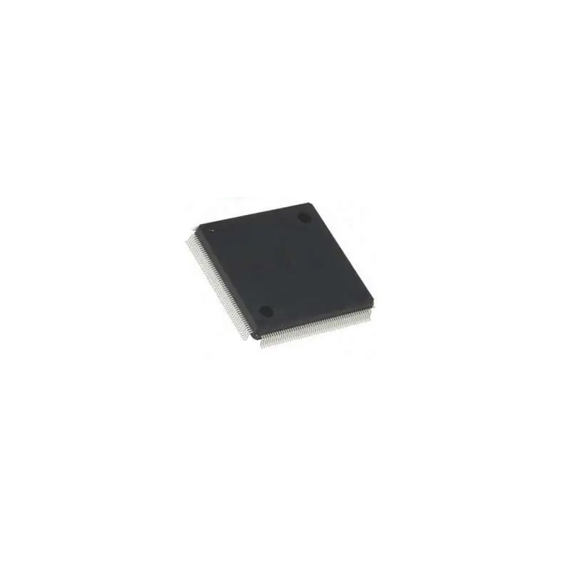
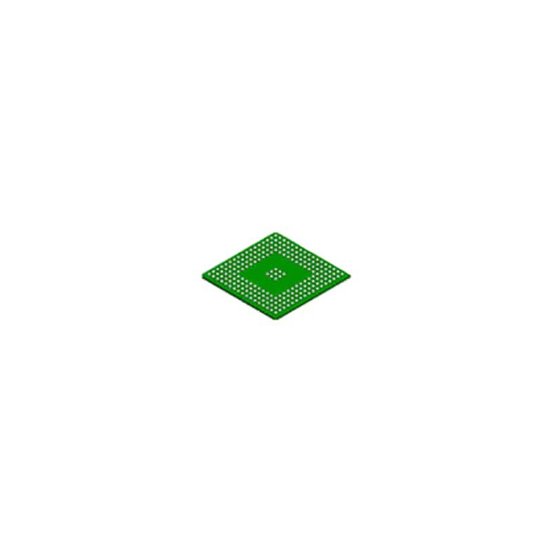
LFXP2-8E-5FTN256C
256-Pin FTBGA Tray
在庫:8,684
- 90日間のアフター保証
- 365日の品質保証
- 正規品保証
- 7*24時間サービス検疫
-
部品番号 : LFXP2-8E-5FTN256C
-
パッケージ/ケース : FTBGA-256
-
コンポーネントの分類 : FPGAs
-
日付シート : LFXP2-8E-5FTN256C データシート (PDF)
概要 LFXP2-8E-5FTN256C
The LFXP2-8E-5FTN256C is a cutting-edge FPGA from Lattice Semiconductor, designed for high-performance and low-power applications. With 8,192 LUTs and 193 user I/Os, this device offers ample resources for complex designs. Its 256-pin FBGA package ensures robust connectivity and reliability, making it suitable for a wide range of industrial and commercial applications. The FPGA operates at a 1.2V core voltage and supports various I/O standards, including LVCMOS, LVTTL, and LVDS, providing flexibility for different interface requirements. Additionally, the inclusion of PLLs, block RAM, and dedicated multipliers enhances signal processing capabilities, making it ideal for data manipulation tasks. Programmed using the user-friendly Lattice Diamond design software, this FPGA offers an efficient development and implementation process, ensuring smooth integration into diverse systems. With its advanced features and high level of programmability, the LFXP2-8E-5FTN256C is a reliable choice for engineers and developers seeking a versatile and powerful FPGA solution
主な特長
- Fully supports PowerPC™ 60x bus protocol, include PowerPC 603, 604, 740, 750 and 8260.
- Supports up to eight PowerPC bus masters with unlimited slave device support.
- Supports two outstanding bus accesses.
- Supports address only transfer and address bus retry.
- Independent address bus and data bus tenure with separate bus grant and data bus grant.
- Option for fixed priority assignment or rotating priority scheme.
- Designed for ASIC or programmable logic device implementations in various system environments.
- Fully static design with edge triggered flip-flops.
- Optimized for ispXPGA product family.
仕様
以下は、選択された部品の特性やカテゴリーに関する基本的なパラメータである。
| Product Category | FPGA - Field Programmable Gate Array | RoHS | Details |
| Series | LFXP2 | Number of Logic Elements | 8000 LE |
| Adaptive Logic Modules - ALMs | 4000 ALM | Embedded Memory | 221 kbit |
| Number of I/Os | 201 I/O | Supply Voltage - Min | 1.14 V |
| Supply Voltage - Max | 1.26 V | Minimum Operating Temperature | 0 C |
| Maximum Operating Temperature | + 85 C | Mounting Style | SMD/SMT |
| Package / Case | FTBGA-256 | Brand | Lattice |
| Distributed RAM | 18 kbit | Embedded Block RAM - EBR | 221 kbit |
| Height | 1.25 mm | Length | 17 mm |
| Maximum Operating Frequency | 311 MHz | Moisture Sensitive | Yes |
| Number of Logic Array Blocks - LABs | 1000 LAB | Operating Supply Voltage | 1.2 V |
| Product Type | FPGA - Field Programmable Gate Array | Factory Pack Quantity | 90 |
| Subcategory | Programmable Logic ICs | Total Memory | 239 kbit |
| Width | 17 mm | Unit Weight | 0.038449 oz |
保証と返品
保証、返品、および追加情報
-
QAと返品ポリシー
部品の品質保証: 365 日
返品・返金:90日以内
返品・交換:90日以内
-
配送と梱包
配送: たとえば、FedEx、JP、UPS、DHL、SAGAWA、YTC など。
部品パッケージ保証: 100% ESD 帯電防止機能を備えた当社のパッケージは、高い強度と優れた緩衝機能を備えています。
-
支払い
たとえば、VISA、MasterCard、Western Union、PayPal、MoneyGram、楽天ペイなどのチャネルです。
特定の支払いチャネルの好みや要件がある場合は、当社の営業チームにご連絡ください。

LFXP2-8E-5QN208C
Family: LatticeXP2
LFEC1E-4QN208C
I/O ports facilitate efficient communication and data transfer in high-speed systems
LFXP15C-4FN256C
Field Programmable Gate Array with multiple voltage options
LFECP6E-3FN484C
FPGA device with 768 CLBs, able to operate at 420 MHz, enclosed in a PBGA484 package
LFEC3E-5Q208C
420MHz operating frequency
LFE5U-25F-6BG256C
FPGA - Field Programmable Gate Array ECP5; 24.3K LUTs; 1.1V
LFXP2-5E-5QN208C
Versatile connectivity options with 146 I/O
LFXP2-5E-5TN144I
ROHS 5000 625 TQFP-144(20x20) FPGA

LFXP2-40E-5FN484C
Lead-free Field Programmable Gate Array with 435MHz clock speed, offering 40000 cells in a PBGA484 package dimensions of 23x23mm
LFE5U-85F-6BG381C
It comes in a 381-pin CABGA package and is sold in tray packaging
PIC18F4620-I/ML
High voltage compatibility

EPM7160SLC84-10N
This CPLD utilizes 100MHz CMOS technology and is designed to operate efficiently at a voltage of 5V
STM32F072R8T6TR
MCU 32-bit ARM Cortex M0 RISC 64KB Flash 2.5V/3.3V 64-Pin LQFP T/R

ATMEGA8515-16PI
With its 40-pin DIP package, the ATMEGA8515-16PI offers a robust and reliable solution for embedded projects requiring 8-bit processing power

XC3S1000-4FT256C
Programmable gate array with 1.2 volt operation
MK40DX256VLQ10
32-Bit Cortex-M4 CPU
M2S010-TQG144I
SmartFusion2 FPGA containing 12084 cells and built with 65nm technology, designed to operate at 1.2V with a 144-pin TQFP package
DSP56321VL275
The DSP56321VL275 is a cutting-edge digital signal processor and controller that delivers exceptional processing power and flexibility

R5F10WMGAFB#30
RL78 RL78/L13 Microcontroller IC 16-Bit 24MHz 128KB FLASH 80-LQFP

HD6417709AF133BV
Lead-free 208-pin form factor